|
|
|
|
|
 |
 |
||
|
|
|||
|
|
|
||
|
|
|
MASK WORKS | |
|
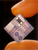
A mask work* is a set of images or templates used in the manufacture of semi-conductor chips. A mask work is a kind of map or blueprint used to design or manufacture a semiconductor chip. The mask work defines the design of the chip in three dimensions, since a semiconductor chip consists of several layers of electronics circuits and elements that are laid down atop one another. The mask work images may be in pictorial or photographic form or broken down into digital numerical form for storage in a computer. In the highly competitive world of computer technology, copyright protection means staying in business. If properly protected and exploited, copyrights in mask works can give your company the edge in both dollars and market share.
|
|||
| *The Statutory Definition: The Semiconductor Chip Protection Act defines a "mask work" as a "series of related images, however fixed or encoded - (A) having or representing the predetermined, three-dimensional pattern of metallic, insulating or semiconducting material present or removed from the layers of a semiconductor chip product; and (B) in which series the relation of the images to one another is that each image has the pattern of the surface of one form of the semiconductor chip product" | |||
|
© Copyright 1995, 2004 Whitelaw Legal Group. All Rights Reserved. Market Intelligence® , The Law of Creativity, The Law of Innovation, The Science of Art, and the design imagery noted ® or are trademarks of the Whitelaw Legal Group |
|||